
RF Antenna PCB Manufacturing High-Performance RF Antenna Printed Circuit Boards
Standard Printed Circuits specializes in the manufacturing of high-frequency RF antenna printed circuit boards for demanding applications where electrical performance, dimensional stability, controlled impedance, and repeatable manufacturing are critical.
Our experience with PTFE, ceramic-filled PTFE, hybrid RF constructions, and other high-frequency laminate systems supports antenna designs used in aerospace, defense, radar, telecommunications, satellite communications, RF communications, test and measurement, and other high-frequency applications.
From prototype and engineering builds through medium-volume production, Standard provides U.S.-based manufacturing support for complex RF antenna PCB designs.

RF Antenna PCB Manufacturing Expertise
RF antenna PCBs require much more than conventional PCB fabrication. Antenna performance can be directly affected by dielectric properties, conductor geometry, copper thickness, dielectric thickness, layer registration, and overall dimensional stability.
Standard's RF PCB manufacturing capabilities include:
- PTFE and ceramic-filled PTFE materials
- Double-sided and multilayer RF antenna PCBs
- Hybrid RF constructions combining high-frequency & conventional materials
- Controlled-impedance circuitry
- Tight conductor width and spacing
- Fine-line circuitry
- Blind and buried vias
- Via-in-pad structures
- Complex mechanical configurations
- Precision copper plating
- Prototype through medium-volume production
- Quick-turn manufacturing
Our engineering and manufacturing teams work with customers to review material selection, stack-up construction, conductor geometry, impedance requirements, tolerances, and manufacturability before production.
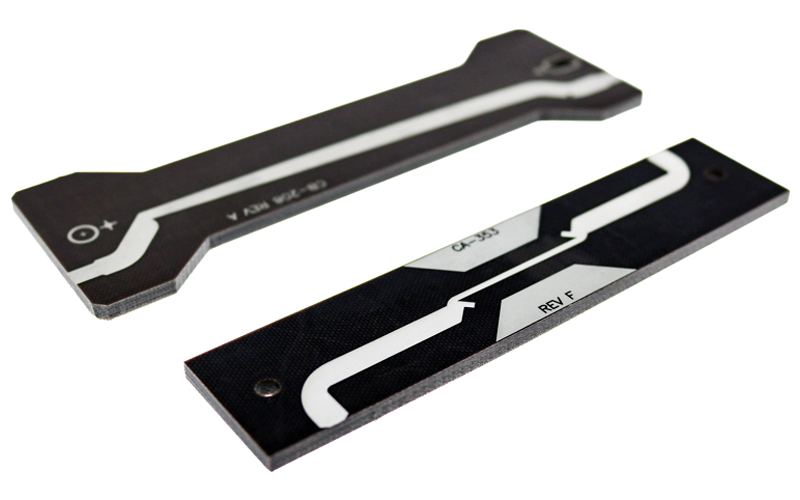
High-Frequency Materials for RF Antennas
Material selection is a critical part of RF antenna performance.
Standard Printed Circuits has extensive experience processing high-frequency materials including PTFE, ceramic-loaded PTFE, TMM, polyimide, polyphenylene oxide, high-performance FR-4, and hybrid material constructions.
We also work with high-frequency laminate systems from leading manufacturers such as Rogers®, Taconic®, and Arlon®.
These materials can provide the controlled dielectric characteristics and low-loss electrical performance required for high-frequency antenna applications.
PTFE Processing for RF Antenna PCBs
PTFE materials provide important electrical characteristics for high-frequency applications, including low dielectric loss, stable dielectric properties, and low moisture absorption.
However, PTFE requires specialized manufacturing processes because its mechanical and surface characteristics differ significantly from conventional FR-4 materials.
Standard's specialized PTFE processing capabilities include:
Sodium Etching
Sodium etching chemically modifies the PTFE surface to promote copper adhesion and support reliable plated-through-hole performance.
Plasma Processing
Plasma etching and surface treatment provide controlled preparation of specialized high-frequency materials and hole walls.
Vacuum Lamination
Vacuum lamination supports complex multilayer and mixed-material antenna constructions where registration, material movement, and dielectric consistency are important.
Precision CNC Drilling and Routing
Precision drilling and routing provide the dimensional control required for complex RF antenna structures and mechanical configurations.
Controlled Impedance & Antenna Geometry
For RF antenna designs, conductor geometry and dielectric characteristics can directly influence electrical performance. Small variations in conductor width, copper thickness, dielectric thickness, or registration can affect impedance and RF performance.
Manufacturing capabilities include:
- Fine lines and spacing down to 2 mils
- Layer-to-layer registration to ±0.001"
- Controlled line-width processing
- Precision copper plating
- Plated-through-hole aspect ratios up to 10:1
- Advanced solder mask registration
Maintaining these characteristics throughout the manufacturing process helps support repeatable electrical performance from prototype through production.
Hybrid RF Antenna PCB Construction
Some antenna assemblies require high-frequency materials only in specific portions of the circuit.
Hybrid RF PCB construction allows high-frequency materials such as PTFE or ceramic-filled PTFE to be combined with FR-4, polyimide, or other conventional PCB materials within the same multilayer construction.
This approach can provide high-frequency performance where required while retaining the mechanical and manufacturing advantages of conventional PCB materials elsewhere in the design.
Standard works with customers to review:
- RF laminate selection
- Conventional laminate selection
- Dielectric thickness
- Copper weights
- Bonding materials
- Controlled impedance requirements
- Layer sequencing
- Copper distribution
- Overall board thickness
- Plated-through-hole requirements
- Registration tolerances
- Lamination requirements
Applications for RF Antenna PCBs
Standard’s RF and microwave PCB manufacturing experience supports antenna applications across a range of demanding industries, including:
- Aerospace and defense
- Radar systems
- Satellite communications
- Telecommunications
- RF communications
- Wireless systems
- Test and measurement equipment
- Industrial electronics
- Research and development
- High-speed electronic systems
U.S. Manufacturing for RF Antenna Applications
Standard Printed Circuits manufactures advanced RF, microwave, PTFE, and hybrid printed circuit boards at its Sherburne, N.Y. facility.
Our manufacturing experience includes specialized high-frequency materials, controlled-impedance processing, precision conductor geometry, multilayer construction, PTFE surface preparation, and complex RF PCB fabrication.
For antenna designs where material selection, dimensional control, and electrical performance are critical, Standard's engineering team can work with your design team to evaluate the PCB construction and manufacturing requirements before production.
Need an RF Antenna PCB?
Contact Standard Printed Circuits to discuss your RF antenna PCB design, material requirements, controlled impedance, stack-up, tolerances, and production requirements.
Request a Quote or contact our engineering team to review your RF antenna application.