
American-Made PTFE / Teflon PCB Manufacturing Specialized U.S. Manufacturing of High-Frequency PTFE Circuit Boards
Standard Printed Circuits specializes in the manufacturing of PTFE printed circuit boards at our Sherburne, N.Y., facility. With decades of experience processing PTFE and other high-frequency laminates, we provide the specialized manufacturing processes, equipment, and engineering expertise required for demanding RF, microwave, aerospace, defense, telecommunications, and high-speed electronic applications.
Commonly referred to as Teflon PCBs, PTFE circuit boards offer excellent electrical performance at high frequencies but require significantly different manufacturing techniques than conventional FR-4 circuit boards.
From prototypes and engineering builds through medium-volume production, Standard provides a reliable U.S.-based source for PTFE and high-frequency PCB manufacturing.
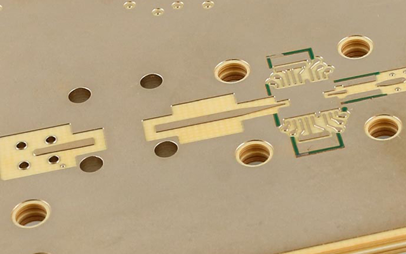
Why Use PTFE for Printed Circuit Boards?
PTFE, or polytetrafluoroethylene, is widely used in high-frequency PCB applications because of its electrical characteristics, including low dielectric loss, stable dielectric properties, low moisture absorption, and excellent performance at microwave and RF frequencies.
These characteristics make PTFE-based materials well suited for applications where maintaining signal integrity and minimizing signal loss are critical.
Typical applications include:
- RF and microwave systems
- Radar and communications equipment
- Antennas
- Power amplifiers
- Filters and couplers
- Satellite communications
- Aerospace and defense electronics
- Test and measurement equipment
- High-speed digital applications
While PTFE offers significant electrical advantages, it also presents unique manufacturing challenges that require specialized PCB fabrication experience.
American PTFE PCB Manufacturing Expertise
PTFE is softer and more mechanically sensitive than traditional FR-4 and requires different approaches to drilling, surface preparation, plating, lamination, imaging, and material handling.
Standard's Sherburne facility has extensive experience processing PTFE, ceramic-filled PTFE, and other high-frequency laminate systems from leading material manufacturers including Rogers®, Taconic®, and Arlon®.
Our PTFE PCB capabilities include:
- Double-sided PTFE PCBs
- Multi-layer PTFE constructions
- Ceramic-filled PTFE materials
- Hybrid PTFE/FR-4 constructions
- Mixed dielectric stack-ups
- Controlled impedance
- Tight controlled line widths
- Fine-line circuitry
- Plated through holes
- Blind and buried vias
- Complex routing and mechanical features
- Prototype through medium-volume manufacturing
- Quick-turn production
Our engineering team works with customers before manufacturing to review material selection, stack-up, tolerances, conductor geometry, and other design characteristics that can affect both manufacturability and electrical performance.
Understanding Laminate Movement During Multi-layer Lamination
One of the most critical challenges in manufacturing multi-layer PTFE and high-frequency printed circuit boards is understanding how each laminate will move during the lamination process.
Unlike conventional FR-4 materials, PTFE and other high-frequency laminates can experience different levels of dimensional change in the X and Y directions when exposed to the heat, pressure, and cooling cycles of a multi-layer lamination press. Ceramic-filled PTFE, unfilled PTFE, bonding materials, copper weights, and hybrid constructions can all behave differently during this process.
Achieving precise layer-to-layer registration requires more than accurate tooling. It requires experience understanding and predicting how a specific laminate and construction will behave throughout the complete lamination cycle.
Standard's manufacturing team uses its experience with high-frequency materials to account for material movement, scaling, artwork compensation, stack-up construction, press parameters, and registration requirements before the multi-layer enters the lamination press.
This becomes particularly important with complex PTFE multi-layers and hybrid constructions, where different materials within the same PCB may expand, contract, or respond differently to temperature and pressure.
By understanding these laminate movement characteristics and applying the appropriate compensation before lamination, Standard can maintain the tight layer-to-layer registration required for demanding RF and microwave designs.
For high-frequency multi-layer PCBs, the objective isn't simply to laminate the layers together. It is to understand where each layer will be after lamination and engineer the manufacturing process accordingly.
That combination of material knowledge, process control, and decades of PTFE manufacturing experience is a critical part of producing repeatable, high-reliability multi-layer RF and microwave circuit boards.
Specialized PTFE Surface Preparation
One of the most important differences between PTFE and conventional PCB materials is the preparation required to achieve reliable copper adhesion and plated-through-hole performance.
Standard maintains specialized processes for PTFE manufacturing, including sodium etching and plasma processing.
Sodium Etching
The naturally non-stick surface characteristics of PTFE make conventional PCB surface preparation inadequate for many applications. Sodium etching chemically modifies the PTFE surface to promote adhesion between the material and subsequently deposited copper.
Proper surface preparation is especially important for achieving reliable plated-through-hole structures and long-term PCB performance.
Plasma Processing
Standard also utilizes plasma etching and surface treatment for specialized materials and constructions. Plasma processing provides controlled surface preparation and hole-wall conditioning without relying on conventional mechanical preparation techniques.
Having these processes available is an important part of consistently manufacturing high-reliability PTFE circuit boards.
Controlled Impedance & Tight-Tolerance Manufacturing
PTFE circuit boards are frequently used in applications where impedance and signal performance are directly influenced by conductor geometry, dielectric thickness, copper thickness, and material properties.
This makes manufacturing process control especially important.
Standard's Sherburne manufacturing capabilities include fine lines and spacing down to 2 mils, layer-to-layer registration to ±0.001", controlled line-width capabilities, precision copper plating, and plated-through-hole aspect ratios up to 10:1.
Our precision etching processes provide tight control of conductor geometry to help maintain the electrical characteristics required by high-frequency PCB designs.
Need a PTFE / Teflon PCB?
Contact Standard Printed Circuits to have our engineering team review your design, impedance requirements, and tolerances.
Request a Quote