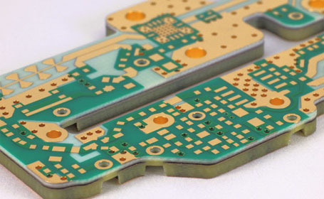
Consisting of multiple laminates and differing dielectric constants, this multilayer (displayed above) is a mixed-dielectric printed circuit board which was manufactured by Standard Printed Circuit, Inc. for the Aerospace Industry. Beginning with Inventory, all the correct materials were pulled and checked against customer requirements and specifications.
Initially, all innerlayers were drilled, imaged, and etched. The innerlayers then proceeded to Lamination where they were pressed into panels using low Dk bonding films. After lamination and cool-down, the panels moved to drilling where all primary holes were drilled. To prepare the hole walls for Direct Metallization, the panels were processed through Plasma and Sodium etching.
After DMS, the outer layers of the panels were imaged, copper plated, solder plated, and etched. Trace widths had to be controlled to +/- .0005″ to provide the end product with proper electrical characteristics. A Liquid Photoimageable (LPI) soldermask was applied, followed by a ENIG (Electroless Nickel Immersion Gold) final finish. Using a number of product evaluation techniques, including flying probe testing, we ensured that this PCB met with all client product requirements. By the end of this project, our company manufactured 75 multilayer, mixed- dielectric printed circuit boards for this aerospace customer, vacuum packaging and shipping all completed items to their facility in Northeastern US.

