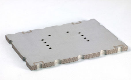
This multi-layer, high-frequency coupler, shown above, is used within a communications application for the telecom industry. Combining a variety of manufacturing services, Standard Printed Circuit Boards built 25 of these couplers for our client. We first sheared the material to size and fabricated the parts’ inner layers, which were then laminated. Our CNC drill formed all primary holes, as well as holes for plated castellations. A mixture of sodium and plasma etching was performed to prep the holes’ walls. Direct metallization was also carried out, using a polymer to produce conductive drilled hole walls.

After plating the couplers in copper, we etched the PCB, removing all surplus copper material. In addition, we endowed the parts with an immersion tin finish and applied all silkscreen graphics. The finished couplers measured 1.25″ x 1″, and possessed 6 separate layers. We also evaluated the product to ensure that all parts fulfilled client specifications.

The finished units were vacuum packed and shipped to our consumer in New York City. Meeting IPC-6018A Microwave End Product Board Inspection and Test standards, our couplers exceeded customer expectations for both design and quality.

Multi-layer High Frequency Coupler Highlights

Product Description
This Multi-Layer High-Frequency Coupler is used within a communications application.
Capabilities Applied/Processes
Shearing
  • Cut Material To Size
Inner layer Fabrication (Image, Etch)
Multilayer Lamination
CNC Drilling
  • Drill out primary holes and holes for plated castellations
Deburring
Hole Wall Prep
  • Plasma Etch
  • Sodium Etching
Direct Metallizationul
  • Conductive polymer
Photolithography
Platingul
  • Copper, Solder
Etching
Silkscreening (Legend and Nomenclature)
Immersion Tin Finish
Final Fabrication
  • Routing to final shape and size (including creating burr-free plated castellations)
Packaging - Vacuum packed
Equipment Used
CNC Driller
CNC Router
Etcher
Exposure, Developer
Plasma Etch
Vacuum Lamination Press.
Overall Part Dimensions
Layers: 6
Length: 1.25"
Width: 1"
Tightest Tolerances
±.001 For Line Widths
Material Used
Ceramic Filled PTFE
Estimated Part Weight
10 Grams
In process testing performed
Cross Section Analysis
Full Electrical Testing
Line Width Verification
Industry for Use
Telecom
Quantity Manufactured
7
Delivery Location
Metro New York Area
Standards Met
IPC-6018 Microwave End Product Board Inspection and Test
Product Name
Multi-Layer High Frequency Couplers